产品中心

CLB30110时钟驱动 可替换cdclvc1310 Au5410 LMK00101 PI6C49X0210 8L30110 8L30210 PI6C49X0210-A
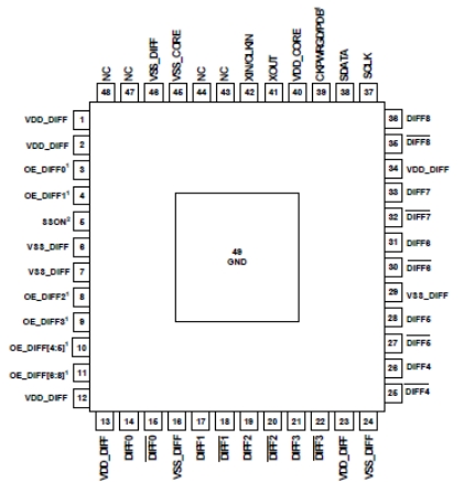
The CLB30110 is a low skew, 1-to-10 LVCMOS/LVTTL Fanout Buffer.
The low impedance LVCMOS/LVTTL outputs are designed to drive 50Ω series or parallel terminated transmission lines.
The CLB30110 is characterized at full 3.3V and 2.5V, mixed 3.3V/2.5V, 3.3V/1.8V, 3.3V/1.5V, 2.5V/1.8V, 2.5V/1.5V and 1.8V/1.5V
output operating supply modes.
The input clock is selected from two differential clock inputs or a crystal input.
The differential input can be wired to accept a single-ended input. The internal oscillator circuit is automatically disabled if the crystal
input is not selected.
Features
• Ten LVCMOS / LVTTL outputs up to 250MHz
• Differential input pair can accept the following differential input levels: LVPECL, LVDS, HCSL
• Crystal Oscillator Interface
• Crystal input frequency range: 8MHz to 50MHz
• Output skew: 20ps (typical)
• Additive RMS phase jitter: 40fs (typical)
• Power supply modes:
Core/Output
3.3V/3.3V 3.3V/2.5V 3.3V/1.8V 3.3V/1.5V 2.5V/2.5V 2.5V/1.8V
2.5V/1.5V 1.8V/1.8V 1.8V/1.5V
• -40°C to 85°C ambient operating temperature
• Lead-free (RoHS 6) packaging
• Supports 105°C board temperature operation

 客服邮箱
客服邮箱 在线客服
在线客服 扫描关注信立诚微信
 扫描关注信立诚微博
